
BATCH ATOMIC-LAYER DEPOSITION
Batch atomic-layer deposition equipment

Batch atomic-layer deposition equipment
Furnace ALD rather than a single-wafer ALD SKU catalog
AI & HPC · Data Center · Consumer Electronics
Public source
Batch ALD is a publicly named Kokusai Electric deposition technology.
Silicon Showcase illustrative visual
Illustrative representation based on publicly available technical information.
Kokusai Batch ALD combines atomic-layer deposition with multi-wafer batch furnaces for 3D device films.
Official Kokusai business pages describe batch ALD as combining ALD step coverage with batch productivity for deeper, narrower 3D structures. This listing records Batch ALD rather than every Kokusai furnace SKU.
Key characteristics associated with this technology.
Batch atomic-layer deposition equipment
Furnace ALD rather than a single-wafer ALD SKU catalog
Not a treatment-only listing
Explore other semiconductor technologies.
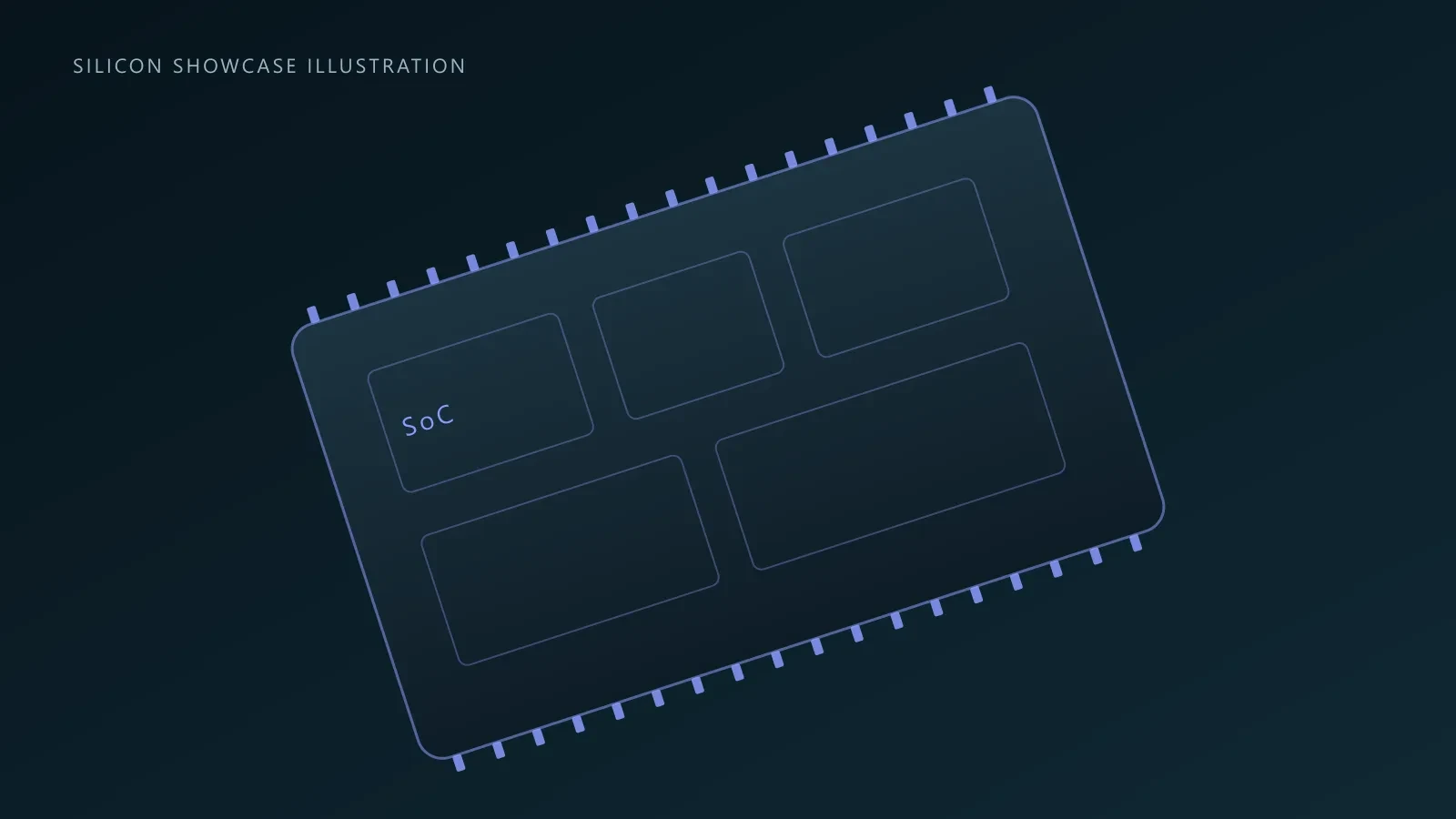
Ultra-low-power connected-device system-on-chip that Sensesemi describes with wireless connectivity, a microcontroller, and an edge AI accelerator.
Consumer ElectronicsMedicalView Technology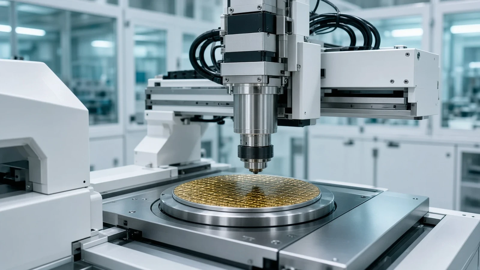
Kulicke & Soffa APTURA is a thermo-compression bonder for advanced packaging, not a wire bonder catalog and not OSAT assembly.
AI & HPCData CenterView Technology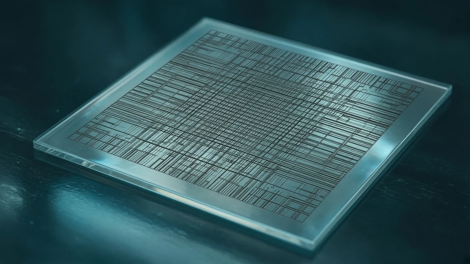
Photronics advanced IC photomasks are lithography reticles for integrated circuits, not a foundry node and not FPD masks.
AutomotiveAI & HPCView Technology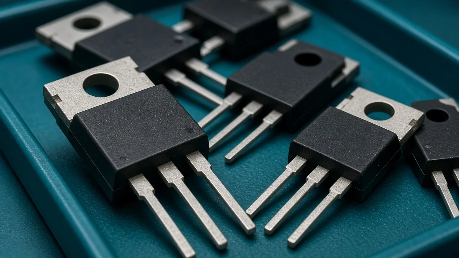
AlphaSGT is Alpha and Omega’s shielded-gate trench MOSFET technology, not a GaN HEMT and not a power-module substrate.
AI & HPCData CenterView Technology


