
GAAS AND GAN
GaAs and GaN foundry processes

GaAs and GaN foundry processes
Compound-semiconductor foundry rather than a catalog MMIC
Data Center · Telecommunications · Aerospace & Defense
Public source
III-V Foundry Process Platform is a publicly named MACOM MESC foundry offering covering GaAs pHEMT/mHEMT and GaN-on-Si HEMT processes.
Silicon Showcase illustrative visual
Illustrative representation based on publicly available technical information.
MACOM’s European Semiconductor Center publishes GaAs and GaN III-V foundry processes for microwave and mmWave devices.
Official MACOM process pages describe device processes for LNA, PA and T/R chips from microwave through mmWave. The listing is parked in Photonics because Foundry / Process does not yet exist; it is not dumped into Design & IP. This listing records the III-V foundry platform rather than MACOM’s catalog MMICs.
Key characteristics associated with this technology.
GaAs and GaN foundry processes
Compound-semiconductor foundry rather than a catalog MMIC
Parked in Photonics pending a Foundry / Process area
Explore other semiconductor technologies.

NB-IoT system-on-chip that WiSig Networks describes as a 3GPP-compliant device with satellite non-terrestrial-network support and edge AI.
TelecommunicationsIoTView Technology
Saankhya Labs' Pruthvi-3 is a software-defined radio chipset series spanning baseband, mobile-receiver and modulator devices.
TelecommunicationsIoTView Technology
Aheesa's Vihaan-I is a RISC-V networking SoC for fiber broadband. First-pass silicon was announced in 2026, with production tape-out targeted for 2027.
AutomotiveIndustrialView Technology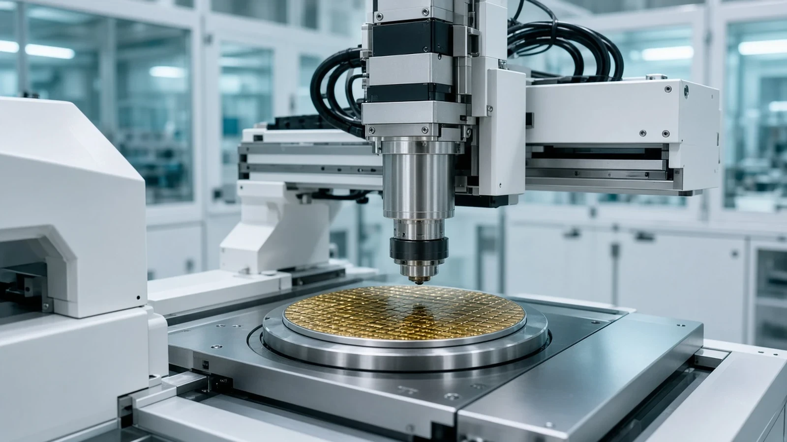
Kulicke & Soffa APTURA is a thermo-compression bonder for advanced packaging, not a wire bonder catalog and not OSAT assembly.
AI & HPCData CenterView Technology
