
HBM4 STACK WITH
HBM4 stack with 2,048 I/O terminals
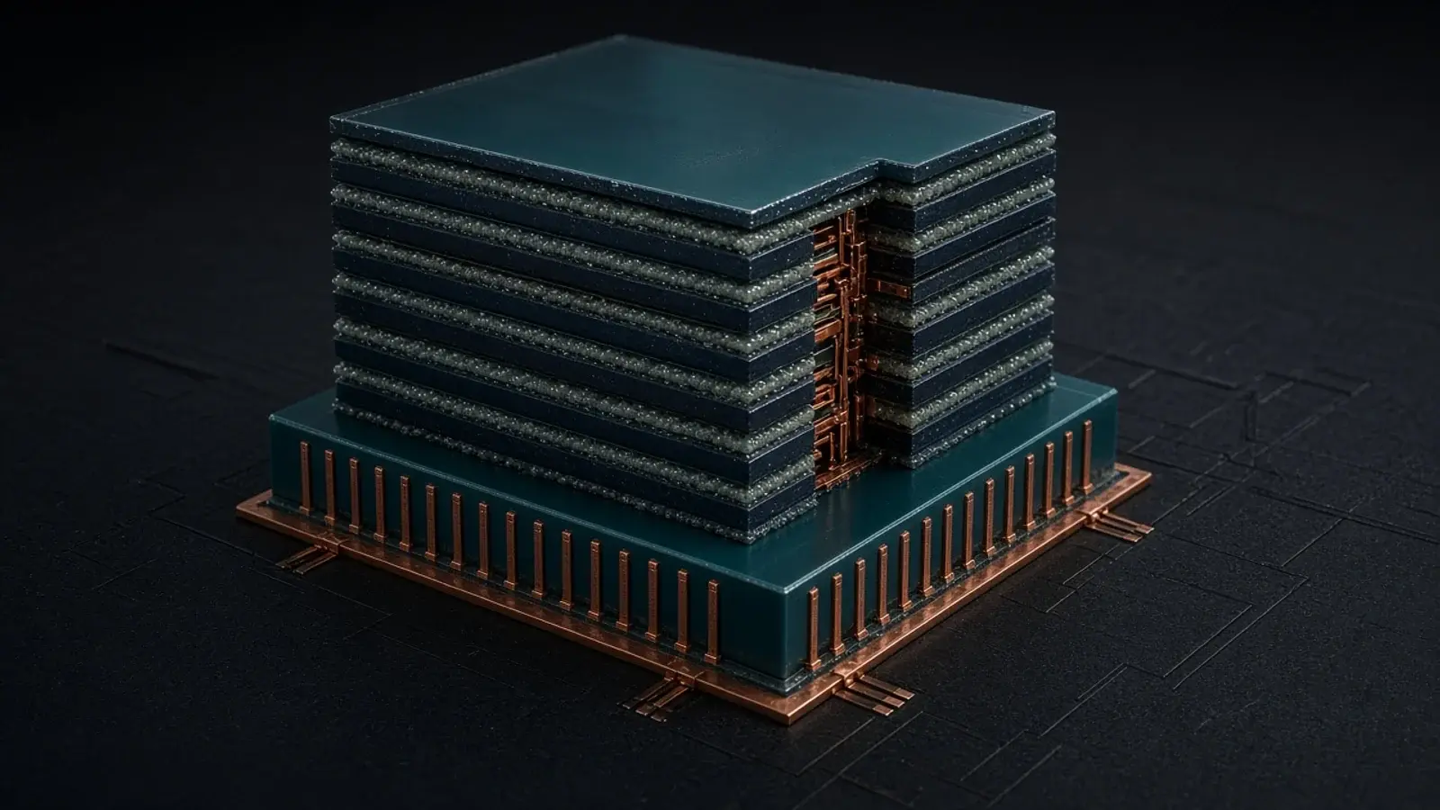
HBM4 stack with 2,048 I/O terminals
Advanced MR-MUF molding between DRAM dies
AI & HPC · Data Center
Public source
SK hynix HBM4 is a publicly named high-bandwidth DRAM stack.
Silicon Showcase illustrative visual
Illustrative representation based on publicly available technical information.
SK hynix HBM4 doubles I/O to 2,048 terminals, claims >10 Gbps and more than 40% better power efficiency versus the prior generation, and uses Advanced MR-MUF to stack DRAM with warpage control and heat dissipation.
Official SK hynix newsroom materials describe HBM4 with 2,048 I/O terminals, speeds above 10 Gbps, more than 40% better power efficiency versus the prior generation, and Advanced MR-MUF stacking for warpage control and heat dissipation. A 19 March 2025 newsroom post describes 12-layer HBM4 samples. This listing records SK hynix’s HBM4 and MR-MUF stack, not HBM3E as a second row. Samsung HBM4 and Micron HBM are other vendors’ implementations of the same device class. Layer counts and bandwidth figures should be confirmed on SK hynix’s current newsroom and product pages.
Key characteristics associated with this technology.
HBM4 stack with 2,048 I/O terminals
Advanced MR-MUF molding between DRAM dies
Official materials describe 12-layer samples and mass-production readiness
Distinct from Samsung HBM4 stacking and Micron HBM devices
Explore other semiconductor technologies.
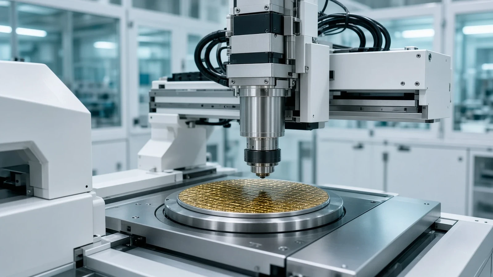
Kulicke & Soffa APTURA is a thermo-compression bonder for advanced packaging, not a wire bonder catalog and not OSAT assembly.
AI & HPCData CenterView Technology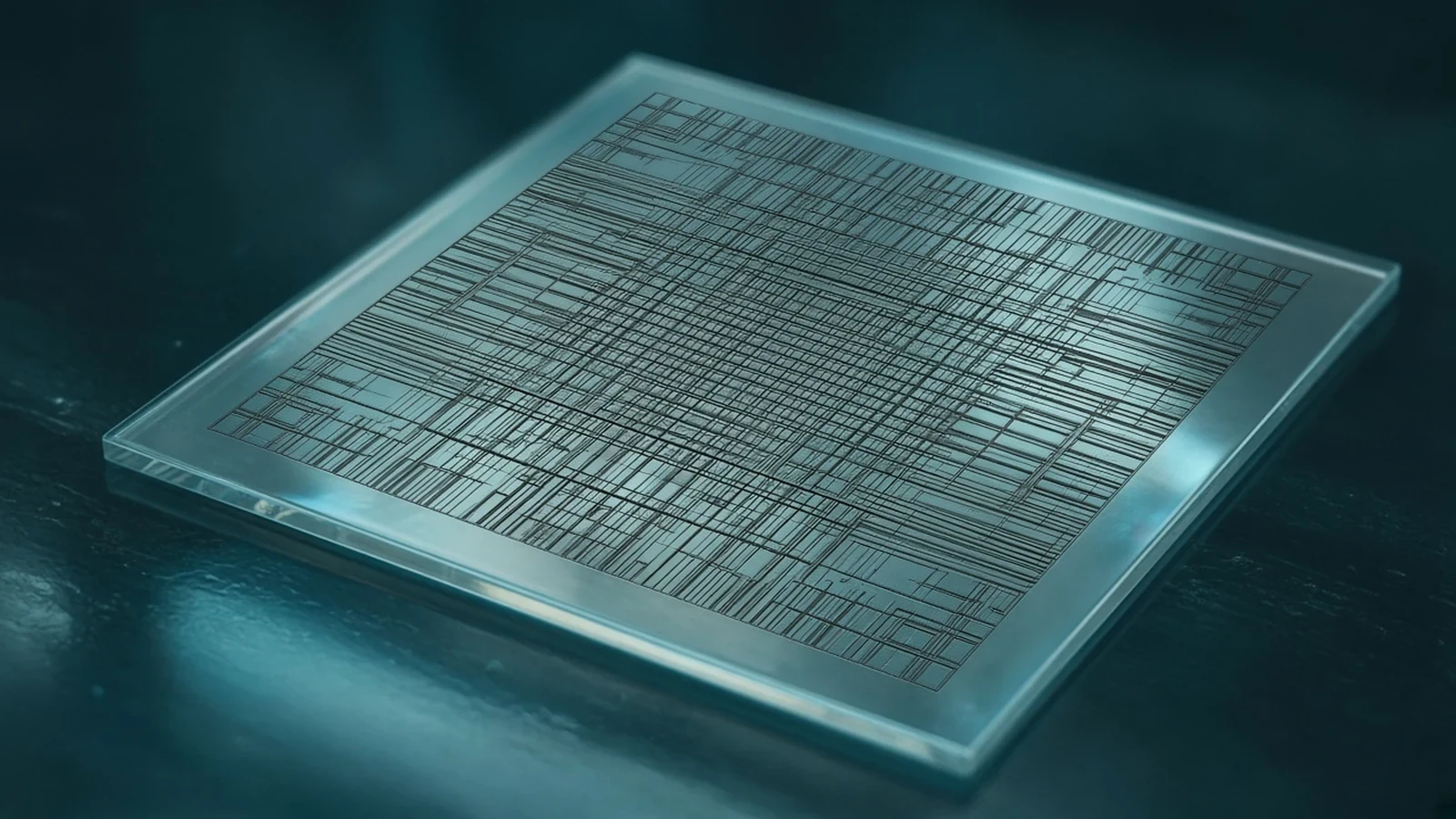
Photronics advanced IC photomasks are lithography reticles for integrated circuits, not a foundry node and not FPD masks.
AutomotiveAI & HPCView Technology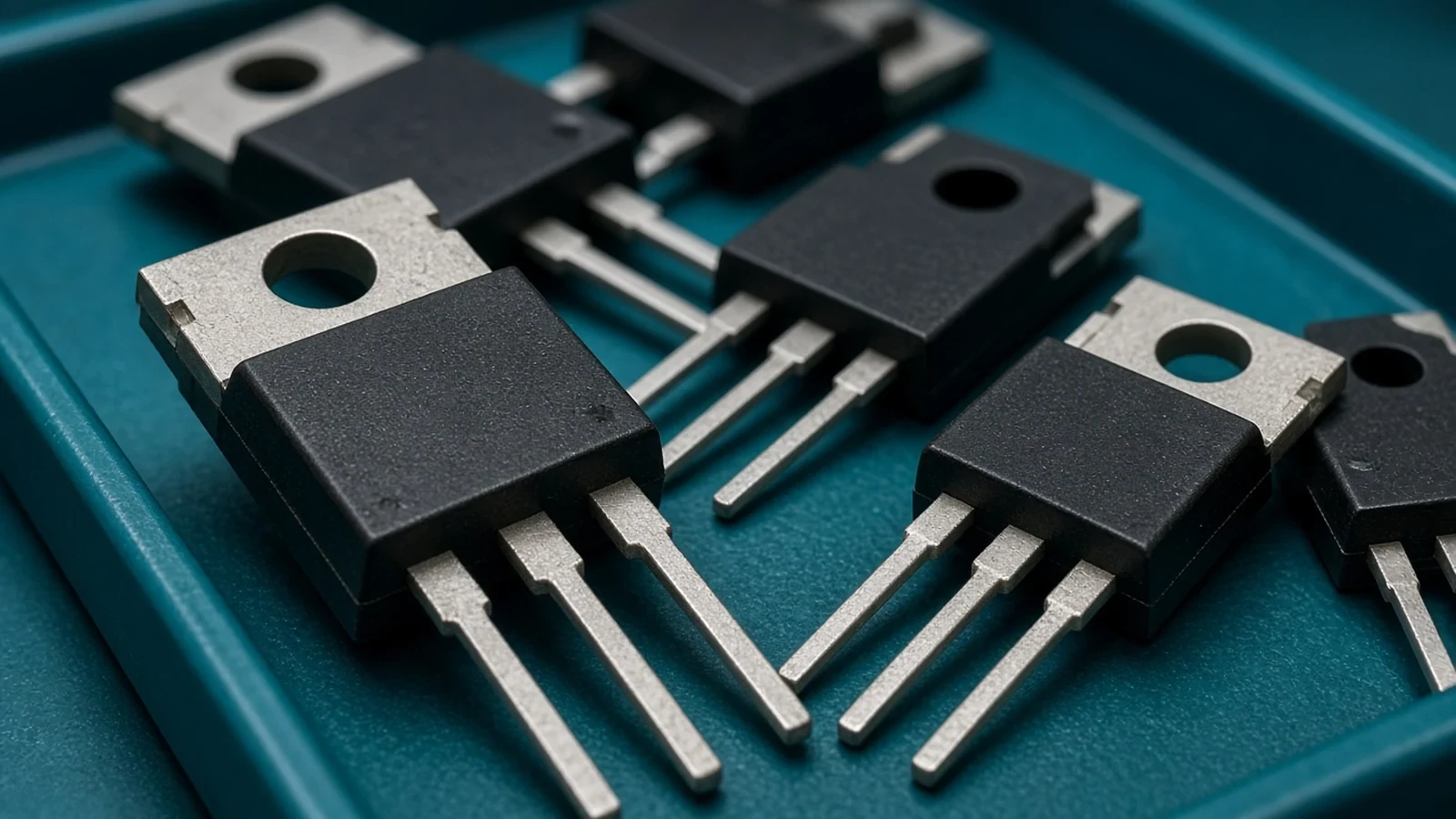
AlphaSGT is Alpha and Omega’s shielded-gate trench MOSFET technology, not a GaN HEMT and not a power-module substrate.
AI & HPCData CenterView Technology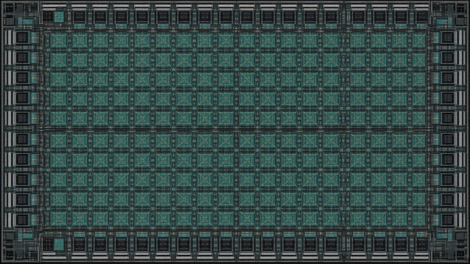
QuickLogic Australis is embedded FPGA IP, not a standalone FPGA chip and not a foundry process.
AI & HPCIndustrialView Technology


